Table Of Content
The number pales in comparison to their NL peers, which routinely come in millions or even billions of sentence pairs. One group of approaches is to introduce constrained natural language (CNL) to formalize the specification drafting, followed by a template-based translation engine. This approach requires significant upfront investment in developing a powerful CNL syntax and a comprehensive compiler/template system to ensure it is powerful enough to address most of the requirements encountered in functional verification. Furthermore, it burdens developers with learning an additional language, which prevents the idea from becoming widely accepted. Complete solutions for the design and manufacturing of printed circuit boards and multi-board electronic systems.
PCB Electronic Design Automation Tools
In all cases, a dedicated hardware model of the circuit will perform far faster than a software program executing the same model. This dramatic increase in speed is often required to complete various tasks in reasonable amounts of time (hours to days vs. weeks to months). The two primary delivery vehicles for EDA hardware are emulation and rapid prototyping. Developers working on IC design can be most productive when the proper tools are provided.
Learn
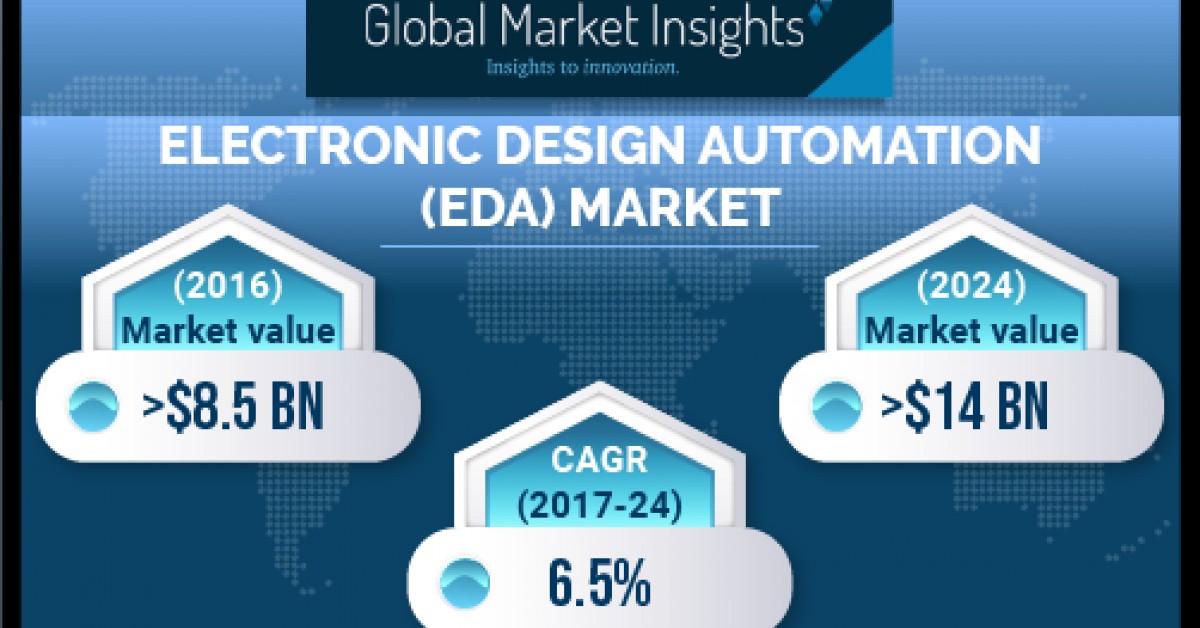
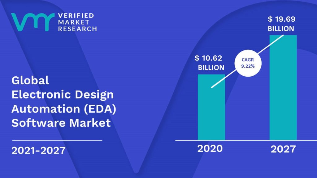
Although the global EDA market was valued at only around $10 billion in 2021, making it a small fraction of the $595 billion semiconductor market, it’s of unique importance to the entire supply chain. Leverage our extensive 30+ industry experienceto help you take your skills to the next level. Connect and streamline your systems for a complete digital thread of your design. Comprehensive platform for concept-to-production design, management, and governance. Semiconductor IP is also part of the EDA market segment and Synopsys offers the industry’s broadest IP portfolio.
Get the latest updates fromMIT Technology Review
AMD processor core count per socket is also the highest in the x86 industry today. Sarita Adve is the Richard T. Cheng Professor of Computer Science at the University of Illinois Urbana-Champaign where she directs IMMERSE, the Center for Immersive Computing. Her research interests span the system stack, ranging from hardware to applications. Her work on the data-race-free, Java, and C++ memory models forms the foundation for memory models used in most hardware and software systems today. Her group released the ILLIXR (Illinois Extended Reality) testbed, an open-source extended reality system and research testbed, and launched the ILLIXR consortium to democratize XR research, development, and benchmarking.
Access this chapter
Even today, 8 of the top 10 systems (Green500 Nov/2023 rankings) are all based on AMD EPYC – a testament to our goals to make the most efficient compute engines. Here, we'd like to share how AMD IT uses our own technology to help advance our design engineers’ products. We refer to ourselves as “Customer Zero” - we experience the same challenges that our customer EDA IT environments face, and our internal IT solutions address the same problems. While that could very well be a possible author’s bias, this blog is not intended to highlight the technical excellence of our processors – that theme is effectively addressed by our Marketing and Engineering presentations/blogs/articles. Really interested to see how ML training models can free up verification time while better identify test to hit errors earlier in the process. ML might also help IC developers stay productive with semantic code search, which allows retrieving relevant code by NL queries.
Tessent - Tessent Silicon Lifecycle Management solutions include advanced test, debug, safety & security features and in-life data analytics to meet the evolving challenges of today’s silicon lifecycle. One of the most important aspects of EDA software tool utilization is ensuring that your solution integrates with other software that you use. To ensure smooth integration, it is probably best to partner with an industry leader with a track record of providing successful EDA software solutions for engineers. This dominance stems from the relentless evolution of consumer electronics, characterized by increasing sophistication and the insatiable demand for advanced gadgets like smart TVs and smartphones.
It’s like the CAD software that architects use, except it’s more sophisticated, since it deals with billions of minuscule transistors on an integrated circuit. Design EDA tools take a proposed circuit function and assemble the elements needed to build it. Design EDA tools help teams create the right geometric shapes and give insight into how to connect these integral components. Often overseen by a designer, this process is also referred to as “place and route” or a custom layout. All of these elements can interact with each other in subtle ways, and variation in the manufacturing process can introduce more subtle interactions and changes in behavior.
Chip design is divided into several subdivisions, including RTL writing, functional verification, logic synthesis, formal verification, DFT, layout and route, Sign Off, and layout verification. Because the specific procedures for designing digital and analogue chips differ, different EDA software is also needed. The FDA mainly consists of flat panel display design EDA for panel manufacturers. EDA is also the linchpin of flat panel display circuit design, similar to integrated circuit design. One of the most famous was the "Berkeley VLSI Tools Tarball", a set of UNIX utilities used to design early VLSI systems.
Growth returns to semiconductor and EDA tools M&A markets – for now - Design News
Growth returns to semiconductor and EDA tools M&A markets – for now.
Posted: Sun, 12 Nov 2023 10:35:13 GMT [source]
Working at Scale
For more information on effectively using electronic design automation and how we can help you or your team innovate faster, contact us. However, innovations in manufacturing equipment and techniques have resulted in highly mechanized board fabrication and assembly. Coupled with these manufacturing improvements has been the development of software programs to help engineers design PCBs more reliably and efficiently. While most EDA products are delivered as software, there are some cases where physical hardware is also used to deliver capabilities. This occurs when a large amount of data must be processed during simulation and verification.
Protel, OrCAD, Viewlogic, PowerPCB, Cadence PSD, Mentor's Expedition PCB, Zuken CadStart, Winboard, Windraft, Ivex-SPICE, PCB Studio, TANG, and many others are examples of PCB design tools. Software for PCB manufacturing primarily consists of tools for PCB fabrication and process controls. Semiconductor professionals know that developing chips is complex and expensive.
Within a few years, there were many companies specializing in EDA, each with a slightly different emphasis. EDA workloads require exponentially more compute every year to support the inexorable march of miniaturization and performance efficiency in silicon chips. Year on year, AMD IT is expected to deliver more computation, power efficiency, higher performance and throughput. We do this by introducing newer AMD CPUs into our production environment as soon as we can benchmark them. Electronic Design Automation (EDA) is a critical part of how AMD designs these technologies for the world.

This is especially true as teams incorporate more technology into their global workflows. Teams can proactively defend their organization from IP leakage with geofencing capability from tools like Helix IPLM. Geofencing is a security measure that restricts IP availability by geography, regardless of a user’s access permissions – acting as a virtual perimeter around a given location. In addition to ensuring chip reliability, electronic design automation also allows teams to work faster, saving them time and helping them meet ambitious deadlines. Therefore, it is important to define your PCB design process needs and align these challenges with the capabilities and design enhancements that an EDA tool should have to meet your needs.


No comments:
Post a Comment